At Finar Module we believe that the architecture of power devices needs to consider the entire system, Junction to Heat Sink. As such the packaging (including TIM) needs to provide for rapid and efficient dissipation of the heat created during use of the device. It is also necessary to avoid excessive mechanical stresses due to differential thermal expansion and contraction of the component parts. These excessive stresses tend to adversely affect the electrical performance of the device and ultimately destroy the solder or attach junctions either with the chip or the substrate. The coefficient of thermal expansion (CTE) of copper is around 17.5 parts per million per degree centigrade while the CTE for mono-crystalline silicon is about 4.6 parts per million per degree C. The difference in CTE is the phenomenon called CTE mis-matching and it is this difference that creates powerful forces that lead to problems of reliability. It is these problems that has resulted in the polarization of power device design over the decades and the resulting plateauing of power densities.

CTE MATCHING
FINAR BUFFER at the core of FM Tech.
Finar Buffer is a buffer structure, engineered to provide anisotropic behaviour. This provides CTE MATCHING properties between different materials in power device packaging. Its internal structure can be described as a self-standing, closely packed pin grid array (CPPGA), where the thickness of the pin is small compared to its height (see Figure 1). It is necessarily made using an electrically and thermally conductive material, such as copper.
The density (or high fill-factor) of the CPPGA is a key element of the engineering of Finar Buffer, which in our development has reached over 90% (and can potentially exceed 95%). We underline that a thin and long pin provides improved flexibility in the plane direction and extremely low structural stiffness in the normal direction compared to solder and consequently to the semiconductor and bulk metals.
The CPPGA orientation within the Finar Buffer structure has a strong bias in the normal direction and poor lateral connection between each other. Moreover, the pins do not form a homogeneous structure, they are not straight or in parallel and this further increases the flexibility (see Figure 2).
Put another way Finar Buffer is composed of many strands, loosely connected between each other (remember it is self-standing). The two tips of each strand are attached to the two facing materials forming a compliant interconnect. These strands allow for large displacement between the two tips of each strand. This means that Material A, attached to one side of the Finar Buffer, experiences its own thermal dilatation with little or no stress coming from Material B as the deformed Finar Buffer strand exerts a very low force between the tips.
Likewise the Material B on the other side of the Finar Buffer experiences its own thermal dilatation with little or no stress coming from Material A or the Finar Buffer itself.
This CTE MATCHING ability enormously reduces shear stress and peeling stress and this is how FM Tech provides phenomenal reliability. This feature also enables optimal stacking architecture for thermal spread and simplified design and production, all while still using standard economic materials.
_edited.jpg)


"ZERO ATTACH"
Figure 2
Figure 1
Finar Buffer overcomes the thermal resistance provided by attach layers through a complex 3D attach, in which the FB pins pierce the attach material, which is squeezed into the interstitial spaces between the pins, forming necks around the pin heads (see Figure 3). In this way the pins have virtually a contact level thermal and electrical connection with the facing element. This is “Zero Attach", almost totally neutralizing the thermal resistance of the attach material!! The embedded neck around the FB pins further provides an extremely high adhesion due to the micro-mechanical interlocking. This is valid for any attach material and it has been verified using solder, conductive epoxy resin, epoxy resin, TIM paste.
Any more questions? You're not alone, have a browse in FAQs

Figure 3
KEY TECHNICAL ADVANTAGES:
-
70% Reduction in Thermal Resistance (Rth j-hs)!!
-
50% Increase in Power Density
-
CTE MATCHING Technology
-
Long Lifespan: 180X LESIT
-
Robust and Resistant
-
Can handle high and low temperatures
-
Compatible with Next Gen WBGs
-
30% Reduction in Bill of Materials (Cost)!
-
Stable and traditional materials
-
Simple architecture - Naturally 3D
-
Cost saving Design & Production
-
Removal of Wire Bonding
-
Simple Greener process
The important characteristic of Finar Buffer's "Zero Attach" quality means it can virtually neutralize the thermal or electrical contribution of solder, TIM or other attach and also offers great grip to any embedding material and removes limitations to resin/mold area.
Finar Buffer provides very high thermal conductivity in the normal direction giving unprecedented thermal performance: 70% Reduction in Thermal Resistance (Rth j-hs) for insulated devices like Power Modules and an unimaginable 50% reduction in the un-insulated thermal resistance (Rth j-pcb)!! That's right! Finar Buffer improves the Thermal Resistance even for un-insulated devices.
This enables an increase in power density of up to 50% that can enable huge cost savings by aggressively reducing the chip size, by as much as 50%. Considering that the chip accounts for between 45% and 50% of the BoM, we envisage a total cost saving from FM Tech in the order of 30%!
Finar Buffer provides high flexibility on the plane direction, to manage the join between different materials virtually removing CTE mismatch problems and allowing for unprecedented reliability and life-cycle expectations.
FM Tech is compatible with high temperature devices, even next generation WBGs.
Finar Buffer also has a very high electrical conductivity along the normal direction to minimize electric resistance and allowing for a low inductance structure.
CTE Matching allows the direct application of bulky electrodes to the semiconductor (both sides) as well providing a bond between large, thick copper heat spreaders (and / or electrode) and large substrates.
Used on the top metalization of a chip, FM Tech allows the removal of wire bonding for a full Finar Buffer interconnection between the chip and the leads.
FM Tech permits 3D topologies easily providing a symmetrical thermal path around the semiconductor and double-sided cooling. It also provides endless planar design possibilities to lower stray inductance and operate at higher switching frequency.
Finar Buffer has significant elasticity and compliance capability on the normal direction enabling it to perform as an efficient spring. This also permits high and controlled pressure to be applied on the semiconductor – eventually performing strain profiling in the semiconductor for higher carrier mobility and lower Rdson.
This same characteristic means Finar Buffer has flexible spatial correlation in the plane, enabling it to compensate for poor surface smoothness and poor planarity, both of itself and its facing material, allowing the use of both cheaper production processes for Finar Buffer and cheaper substrates.
SIMPLE BUILDING BLOCKS FOR THE FUTURE: FM TECH
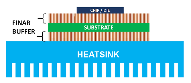

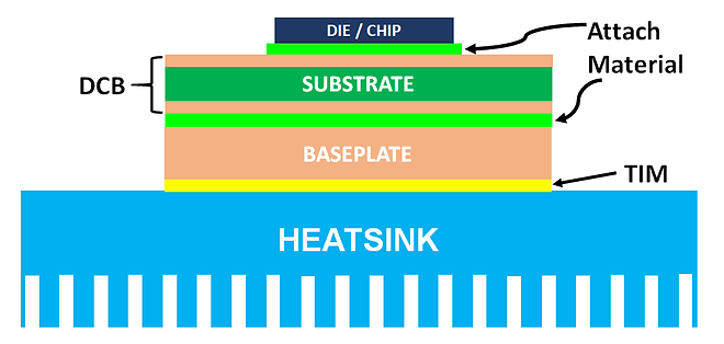
COMPARE WITH THE OLD STANDARD PACKAGE: